时钟切换电路
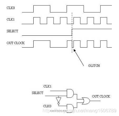
1.MUX时钟切换
这是时钟切换的最简单实现方式,但是这种可能会产生毛刺(glitch),不推荐使用。
2.无毛刺时钟切换
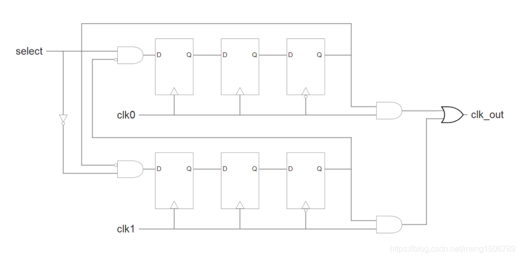
电路图详解:
(1)由于sel至少对于其中一个时钟是异步信号,前面引入两级DFF是为了完成sel信号的跨时钟域。
(2)输入端引入输出反馈确保另一端的控制信号为低电平(另一端的输出关断)时发生切换。
(3)最后一级插入下降沿触发触发器确保切换只发生在时钟为低电平时,避免glitch。
程序实例
clock_switch.v
`timescale 1ns / 1ps

// Company:
// Engineer:
//
// Create Date: 2020/12/19
// Author Name: Sniper
// Module Name: clock_switch
// Project Name:
// Target Devices:
// Tool Versions:
// Description:
//
// Dependencies:
//
// Revision:
// Revision 0.01 - File Created
// Additional Comments:
//


module clock_switch(
    input rst_n,
    input clk0,
    input clk1,
	//async select
	input select,
	output clk_out
);

wire DFF0_in;
wire DFF1_in;
reg [2:0] DFF0_out;
reg [2:0] DFF1_out;

assign DFF0_in = ~DFF1_out[2] & ~select;
assign DFF1_in = ~DFF0_out[2] & select;

always @(posedge clk0 or negedge rst_n)
    if(!rst_n)
        DFF0_out[1:0] <= 2'b00;
    else
        DFF0_out[1:0] <= {

    DFF0_out[0],DFF0_in};

always @(negedge clk0 or negedge rst_n)
    if(!rst_n)
        DFF0_out[2] <= 1'b0;
    else
        DFF0_out[2] <= DFF0_out[1];


always @(posedge clk1 or negedge rst_n)
    if(!rst_n)
        DFF1_out[1:0] <= 2'b00;
    else
        DFF1_out[1:0] <= {

    DFF1_out[0],DFF1_in};

always @(negedge clk1 or negedge rst_n)
    if(!rst_n)
        DFF1_out[2] <= 1'b0;
    else
        DFF1_out[2] <= DFF1_out[1];


wire clk_out0;
wire clk_out1;

assign clk_out0 = clk0 & DFF0_out[2];
assign clk_out1 = clk1 & DFF1_out[2];
assign clk_out = clk_out0 | clk_out1;


endmodule
tb_clock_switch.v
`timescale 1ns / 1ps

// Company:
// Engineer:
//
// Create Date: 2020/12/19
// Author Name: Sniper
// Module Name: tb_clock_switch
// Project Name:
// Target Devices:
// Tool Versions:
// Description:
//
// Dependencies:
//
// Revision:
// Revision 0.01 - File Created
// Additional Comments:
//


module tb_clock_switch;

//input
reg rst_n;
reg clk0;
reg clk1;
reg select;


//output
wire clk_out;


initial
begin
    rst_n = 0;
    clk0 = 0;
    clk1 = 0;
    select = 0;

	#100;
    rst_n = 1;

	#200;
    select = 1;
	#500;
    select = 0;


end

//clock
always #5 clk0 = ~clk0;
always #22 clk1 = ~clk1;


//DUT
clock_switch DUT
(
    .rst_n(rst_n),
    .clk0(clk0),
    .clk1(clk1),
    .select(select),
    .clk_out(clk_out)
);

initial
begin
    $dumpfile("tb_clock_switch.vcd");
    $dumpvars(0,tb_clock_switch);
end

initial #1000 $finish;

endmodule
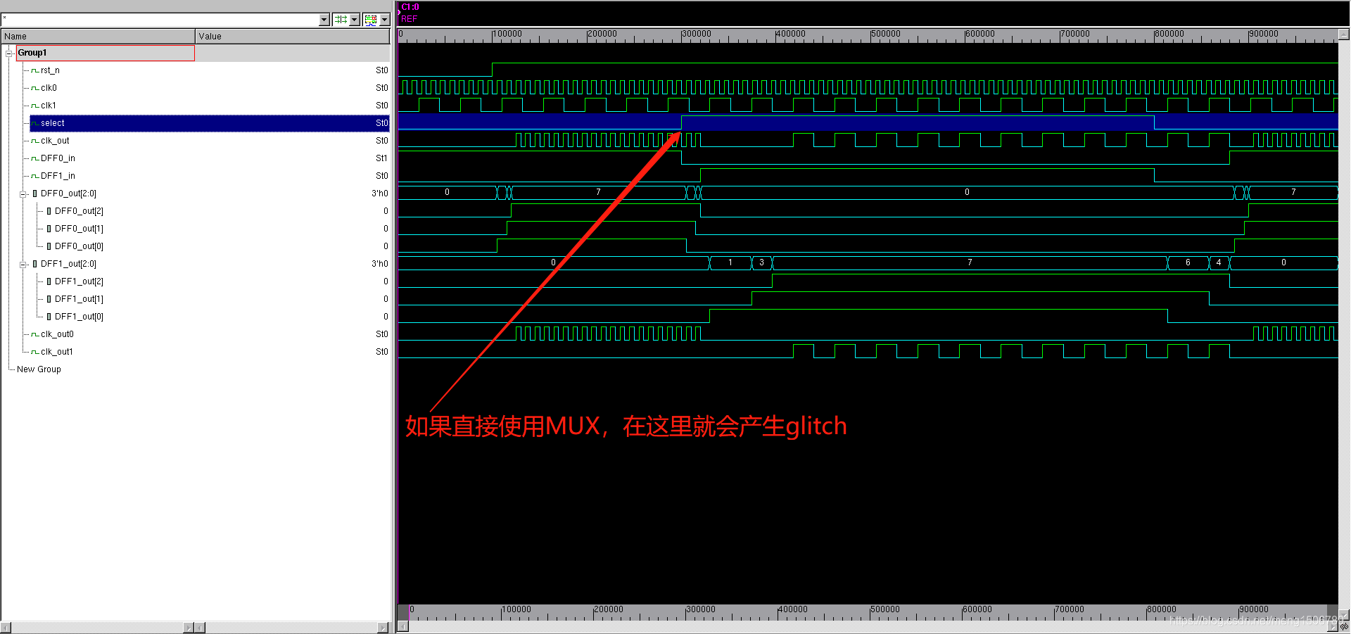
仿真结果
vcs -R clock_switch.v tb_clock_switch.v