基本信号及概念
通信双方及通道
下图为edp规范中的总体框图。通过此框图我们可以了解到:
交互的双方:
1)source device 即 显卡的显示控制部分
2) sink device 即 显示屏
双方间的通道:
1) HPD 即热插拔,通过sink device 传递给source device。虽然有此信号,但是我们采用intel i915驱动支持的显卡,在实际测试过程中,热插拔edp后,connector的链接状态并没有发生变化,而且热插入后,通过modetest命令并不能查询到对应connector的信息。
2) aux channel,通过此通道可以控制背光、读取DPCD 信息以进行main-link的速率协商。
3) main-link ,即图像数据传输通道,支持的速率有:
• 1.62Gbps/lane (RBR)
• 2.7Gbps/lane (HBR)
• 5.4Gbps/lane (HBR2)
• 8.1Gbps/lane (HBR3)
支持的lane数目为x1 x2 x4
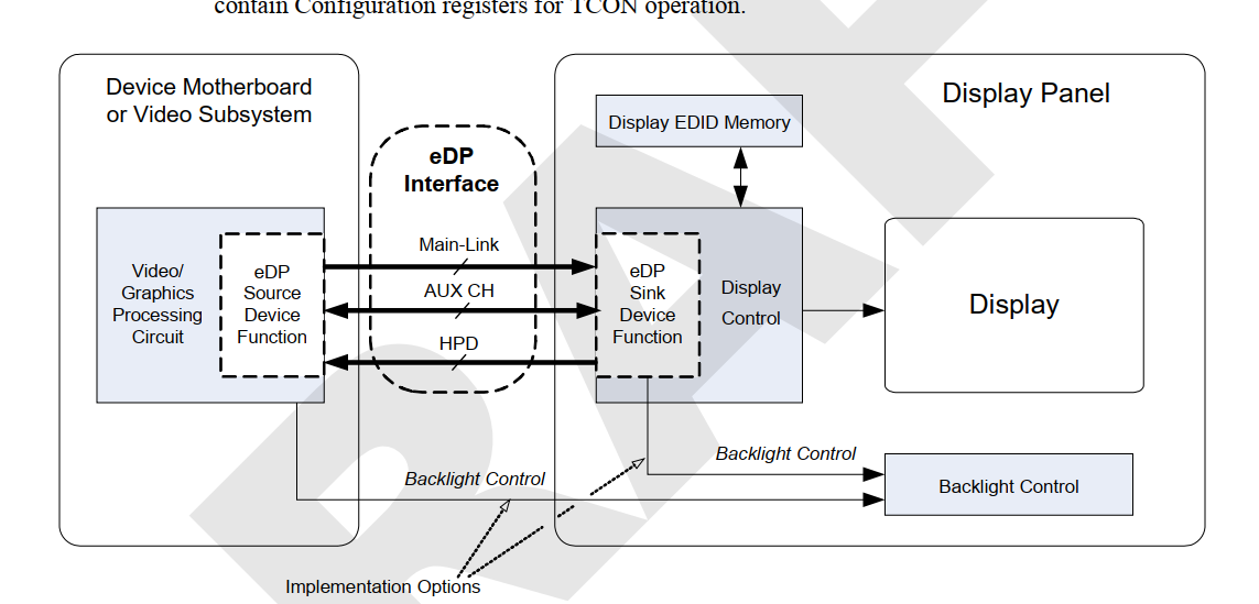
图1 EDP 框图
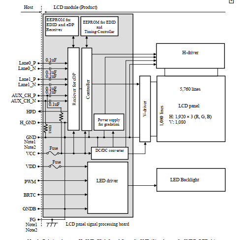
显示屏信号
图2 为某款显示屏的信号.
x2 lane 信号lane0 lan1
aux channel
HPD 信号
PWM 背光控制
此外这里除了EDID,还有timing-controller 通常缩写为TCON。
LINK Traing
Link Training is used to determine the number of lanes supported, link rate, link voltage swing, and pre-emphasis needed to send raw data at the target symbol-error-rate floor of 10-9, over a given cable to a given Sink device
在一个特定的 连接线、显示屏的环境中,决定 link 速率、lane的数目、电压摆幅及预加重值。
也就是电压摆幅和预加重的值也是traing的结果。
eDP defines a Training Table to be used as part of training. VdiffP-P values are mapped into the
Training Table. This enables eDP to use DP Link Training algorithms, while also supporting lower
TX voltage swing and customized voltage swings
Vdiff Training Table
The Source device transmitter implements differential signal voltages (VTX-DIFFP-P) that map into
entries that are logically described in a “training table” format.
The Sink device uses the table structure to request particular adjustments during the training process.
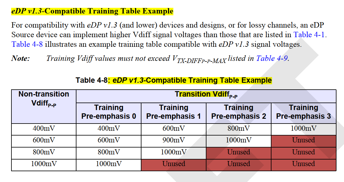
在traing过程中,采用表中不同的电压摆幅和预加重,并最终选择一个。
内核中EDP相关节点及配置
edp_swing
/sys/module/i915/parameters# cat edp_vswing
修改变量:
GRUB_CMDLINE_LINUX_DEFAULT="quiet splash i915.enable_psr=0 i915.edp_vswing=2"
修改完 /etc/default/grub , 需要执行 sudo update-grub 生成 /boot/grub/grub.cfg,重启后生效
The parameter settings (after = sign) can be:
0=default, to do nothing
1=not sure, haven't found answer yet
2=control flicker, which OP used
debug 节点
默认的ubuntu系统带有此节点,有些客户自定配置生成的ubuntu系统则没有此节点。
时钟频率
cat i915_frequency_info
Video Turbo Mode: yes (CPU有turbo mode,这里看起来GPU也存在)
HW control enabled: yes
SW control enabled: no
PM IER=0x00000000 IMR=0xffffffcf, MASK=0x00003ffe
PM ISR=0x00000000 IIR=0x00000000
pm_intrmsk_mbz: 0x80000000
GT_PERF_STATUS: 0x00000000
Render p-state ratio: 0
Render p-state VID: 0
Render p-state limit: 255
RPSTAT1: 0x0a808006
RPMODECTL: 0x00000d92
RPINCLIMIT: 0x00001bd5
RPDECLIMIT: 0x00004fb0
RPNSWREQ: 350MHz
CAGF: 350MHz
RP CUR UP EI: 99 (132000ns)
RP CUR UP: 73 (97334un)
RP PREV UP: 0 (0ns)
Up threshold: 95%
RP CUR DOWN EI: 101 (134667ns)
RP CUR DOWN: 74 (98667ns)
RP PREV DOWN: 0 (0ns)
Down threshold: 85%
Lowest (RPN) frequency: 350MHz
Nominal (RP1) frequency: 350MHz
Max non-overclocked (RP0) frequency: 950MHz
Max overclocked frequency: 950MHz
Current freq: 350 MHz
Actual freq: 350 MHz
Idle freq: 350 MHz
Min freq: 350 MHz
Boost freq: 950 MHz
Max freq: 950 MHz
efficient (RPe) frequency: 350 MHz
Current CD clock frequency: 337500 kHz
Max CD clock frequency: 675000 kHz
Max pixel clock frequency: 675000 kHz
工具命令
edid-decode
1)下载压缩包
apt download edid-decode
dpkg -x edid-decode_0.1~git20191209.e719d04-1build1_amd64.deb ./
2)使用
cat /sys/class/drm/card0-eDP-1/edid |./edid-decode
edid-decode (hex):
00 ff ff ff ff ff ff 00 09 d1 40 7b 36 02 00 00
23 1a 01 03 60 34 1d 78 2e 4e c0 a6 55 50 9c 26
11 50 54 af cf 00 d1 c0 b3 00 95 00 81 80 81 40
81 00 81 c0 71 40 02 3a 80 18 71 38 2d 40 58 2c
45 00 09 25 21 00 00 1e 00 00 00 fd 00 38 4b 1e
51 11 00 0a 20 20 20 20 20 20 00 00 00 fc 00 42
65 6e 51 20 56 5a 32 34 41 30 48 0a 00 00 00 ff
00 45 54 53 38 47 30 30 36 30 30 30 33 48 00 f5
EDID version: 1.3
Manufacturer: BNQ Model 31552 Serial Number 566
Made in week 35 of 2016
Analog display, Input voltage level: 0.7/0.7 V
Sync:
Maximum image size: 52 cm x 29 cm
Gamma: 2.20
DPMS levels: Off
RGB color display
Default (sRGB) color space is primary color space
First detailed timing is preferred timing
Color Characteristics
Red: 0.6494, 0.3320
Green: 0.3154, 0.6113
Blue: 0.1513, 0.0664
White: 0.3125, 0.3281
Established Timings I & II “Established Timings”(内建时序)表示显示器是否支持一些通用时序。
720x400 70.082 Hz 9:5 31.467 kHz 28.320 MHz (IBM)
640x480 59.940 Hz 4:3 31.469 kHz 25.175 MHz (DMT)
640x480 72.809 Hz 4:3 37.861 kHz 31.500 MHz (DMT)
640x480 75.000 Hz 4:3 37.500 kHz 31.500 MHz (DMT)
800x600 56.250 Hz 4:3 35.156 kHz 36.000 MHz (DMT)
800x600 60.317 Hz 4:3 37.879 kHz 40.000 MHz (DMT)
800x600 72.188 Hz 4:3 48.077 kHz 50.000 MHz (DMT)
800x600 75.000 Hz 4:3 46.875 kHz 49.500 MHz (DMT)
1024x768 60.004 Hz 4:3 48.363 kHz 65.000 MHz (DMT)
1024x768 70.069 Hz 4:3 56.476 kHz 75.000 MHz (DMT)
1024x768 75.029 Hz 4:3 60.023 kHz 78.750 MHz (DMT)
1280x1024 75.025 Hz 5:4 79.976 kHz 135.000 MHz (DMT)
Standard Timings
1920x1080 60.000 Hz 16:9 67.500 kHz 148.500 MHz (DMT)
1680x1050 59.954 Hz 16:10 65.290 kHz 146.250 MHz (DMT)
1440x900 59.887 Hz 16:10 55.935 kHz 106.500 MHz (DMT)
1280x1024 60.020 Hz 5:4 63.981 kHz 108.000 MHz (DMT)
1280x960 60.000 Hz 4:3 60.000 kHz 108.000 MHz (DMT)
1280x800 59.810 Hz 16:10 49.702 kHz 83.500 MHz (DMT)
1280x720 60.000 Hz 16:9 45.000 kHz 74.250 MHz (DMT)
1152x864 60.000 Hz 4:3 53.700 kHz 81.624 MHz (GTF)
Detailed mode: Clock 148.500 MHz, 521 mm x 293 mm
1920 2008 2052 2200 ( 88 44 148)
1080 1084 1089 1125 ( 4 5 36)
+hsync +vsync
VertFreq: 60.000 Hz, HorFreq: 67.500 kHz
Display Range Limits
Monitor ranges (GTF): 56-75 Hz V, 30-81 kHz H, max dotclock 170 MHz
Display Product Name: BenQ VZ24A0H
Display Product Serial Number: ETS8G0060003H
Checksum: 0xf5
====================
数据解析
1920 2008 2052 2200 ( 88 44 148) 水平
1080 1084 1089 1125 ( 4 5 36) 垂直
Horizontal: Active Time : 1920 Pixels Blanking Time : 280 Pixels Sync Offset : 88 Pixels Sync Pulse Width: 44 Pixels Border : 0 Pixels Frequency : 67 kHz Vertical: Active Time : 1080 Lines Blanking Time : 45 Lines Sync Offset : 4 Lines Sync Pulse Width: 5 Lines Border : 0 Lines
下角的Timing部分描述了时序的主要参数,含义见下表(软件显示有问题,参数名称显示不完整,表格中的参数也仅对应其在软件中的位置)。H Image、H Border、V Image、V Border几个参数一般用不到,表格中没有列出
参数 |
含义 |
参数 |
含义 |
Pixel |
像素时钟频率 |
Interlaced |
前面打钩表示是隔行显示 |
H Active |
一行中有效的像素 |
V Active |
一场中有效的行数 |
H Blank |
一行中的消隐期长度,单位是像素 |
V Blank |
一场中的消隐期长度,单位是行 |
H sync |
行同步前沿宽度,即从行有效像素结束到行同步开始的像素数 |
V sync |
场同步前沿宽度,即从一场中有效行结束到场同步开始的行数 |
H sync |
行同步信号宽度,单位是像素 |
V sync |
场同步信号宽度,单位是行 |
intel_vbt_decode
apt install intel-gpu-tools
intel_vbt_decode /sys/kernel/debug/dri/0/i915_vbt
VBT header:
VBT signature: "$VBT SKYLAKE "
VBT version: 0x0064 (1.0)
VBT header size: 0x0030 (48)
VBT size: 0x10cc (4300)
VBT checksum: 0xfd
BDB offset: 0x00000030 (48)
BDB header:
BDB signature: "BIOS_DATA_BLOCK "
BDB version: 209
BDB header size: 0x0016 (22)
BDB size: 0x109c (4252)
BDB blocks present:
1 2 3 6 7 8 9 10 12 13 17 18 20 26 27 28
DPCD读取
cat /sys/kernel/debug/dri/0/eDP-1/i915_dpcd
ubuntu 20.4上这个节点不支持
采用intel 工具包中的命令:
dpcd_reg
0x0000: 11 0a 82 01 00 03 01 01 02 00 00 00 00 00 00
0x0070: 00 00
0x0080: 09 00 00 00 00 00 00 00 00 00 00 00 00 00 00 00
0x0100: 0a 82 00 11 11 00 00 00 01 00 00
0x0200: 01 00 77 00 01 01 99 00
0x0600: 01
0x0700: 00
0x0701: 02 00 00 00
0x0720: 00 00 00 00 00 00 00 00 00 0a 14 00 00 00 00 00
0x0732: 00 00
0x2008: 00
GPU工作频率
intel_gpu_frequency --help

intel_gpu_frequency A program to manipulate Intel GPU frequencies.

Usage: intel_gpu_frequency [-e] [--min | --max] [--get] [--set frequency_mhz]

Options:
  -e            Lock frequency to the most efficient frequency
  -g, --get     Get all the frequency settings
  -s, --set     Lock frequency to an absolute value (MHz)
  -c, --custom  Set a min, or max frequency "min=X | max=Y"
  -m  --max     Lock frequency to max frequency
  -i  --min     Lock frequency to min (never a good idea, DEBUG ONLY)
  -d  --defaults  Return the system to hardware defaults
  -h  --help    Returns this
  -v  --version Version

Examples:
   intel_gpu_frequency --get            Get the current and minimum frequency
   intel_gpu_frequency --set 400        Lock frequency to 400Mhz
   intel_gpu_frequency --custom max=750 Set the max frequency to 750MHz

Report bugs to <bugs.freedesktop.org>
获取GPU工作频率
intel_gpu_frequency -g
cur: 350 MHz
min: 350 MHz
RP1: 350 MHz (RP1 是什么意思?)
max: 950 MHz
设置GPU固定工作频率
intel_gpu_frequency -s 500
root@user-Default-string:/home/user# intel_gpu_frequency -g
cur: 500 MHz
min: 500 MHz
RP1: 350 MHz (这个没被修改)
max: 500 MHz
锁定工作频率到有效的频率
intel_gpu_frequency -e
root@user-Default-string:/home/user# intel_gpu_frequency -g
cur: 350 MHz
min: 350 MHz
RP1: 350 MHz
max: 350 MHz
查看GPU资源使用情况
intel-gpu-top
- 156/ 160 MHz; 72% RC6; 0.19 Watts; 556 irqs/s
IMC reads: 804 MiB/s
IMC writes: 119 MiB/s
ENGINE BUSY MI_SEMA MI_WAIT
Render/3D/0 8.83% |████████▍ | 0% 0%
Blitter/0 0.00% | | 0% 0%
Video/0 0.00% | | 0% 0%
VideoEnhance/0 0.00% | | 0% 0%
RC6 : 定义
intel显卡原理
硬件组件

基本构成
pipe A \B \C
transcoder A B C
Timing
DDI
pipe组件
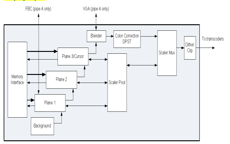
主要包括
plane 3个plane的应用? 怎么确定是否已经启用三个plane
scaler pool scale Mux 缩放
color corection DPST
dither clip 裁剪 不在此次考虑范围内。
CD clock
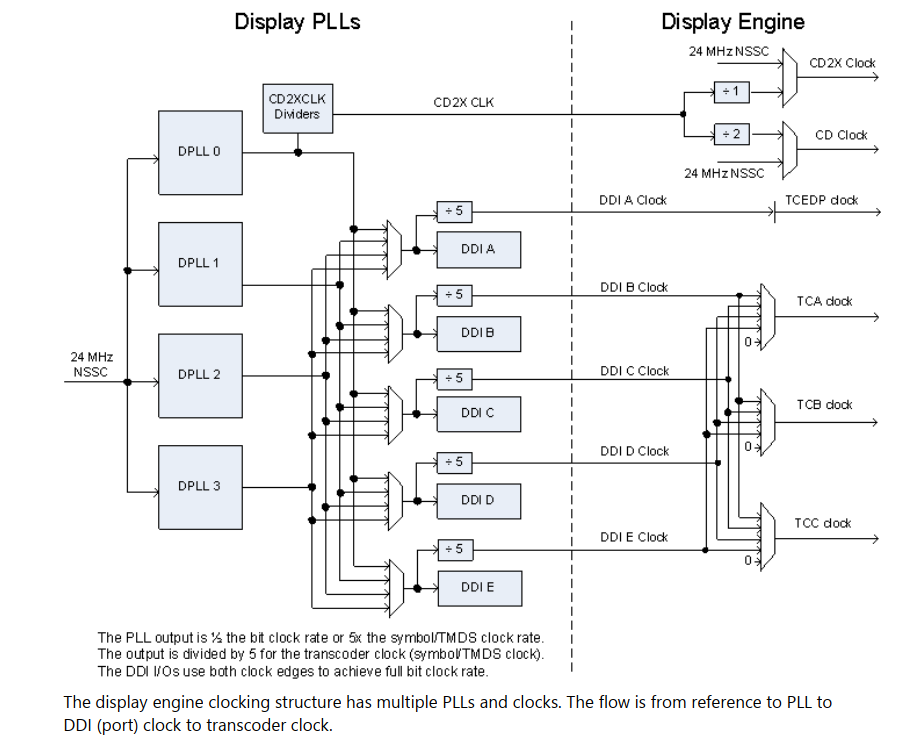
核心显示时钟--包括 1x和2x
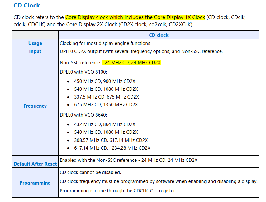
目前系统中采用的337.5MHz 和675MHZ这一组。
Current CD clock frequency: 337500 kHz
Max CD clock frequency: 675000 kHz
Max pixel clock frequency: 675000 kHz
上面这组值应该针对不同的显示屏会有值吧。
配置选择
如何决定选择哪一组?
屏的时钟
上面cd clk /5 即和屏的时钟要对应。 tc是关键词。屏 --symbol tc; 控制器 tcedp clock 、tcA clk等。
数据大小计算
pixel rate
Pixel rate refers to the number of pixels that a GPU can render onto a screen every second.
即GPU 每秒渲染到频率的像素个数。每个像素可能是24位 32位等。
Example pipe pixel rate:
Plane 1 enabled at 32bpp, plane 2 enabled at 16bpp, pipe scaling enabled and down scale amount 1.12,
and CDCLK 450 MHz:
Plane 1 ratio = 1
Plane 2 ratio = 1
Pipe ratio = Minimum[1, 1] = 1
Pipe ratio = 1/1.12 = 0.89
Pipe maximum pixel rate = 450 MHz * 0.89 = 400.5 MHz
内存带宽需求
Example memory bandwidth:
System memory bandwidth available for display = 4000 MB/s
Pipe A - Plane 1 enabled at 32bpp, plane 2 enabled at 16bpp, scaling disabled, pixel rate 148.5 MHz
Pipe B - Plane 1 enabled at 32bpp, scaling disabled, pixel rate 148.5 MHz
Pipe C - Plane 1 enabled at 32bpp, scaling disabled, pixel rate 148.5 MHz
Pipe A - Plane 1 bandwidth = 148.5 * 4 bytes = 594 MB/s
Pipe A - Plane 2 bandwidth = 148.5 * 2 bytes = 297 MB/s
Pipe B - Plane 1 bandwidth = 148.5 * 4 bytes = 594 MB/s
Pipe C - Plane 1 bandwidth = 148.5 * 4 bytes = 594 MB/s
Total display bandwidth = 594 + 297 + 594 + 594 = 2079 MB/s
System memory bandwidth available for display not exceeded
iboost
I_boost increases the I/O current, boosting the swing level. There are three I_boost values, in order of increasing boost; 0x1, 0x3, and 0x7.
I_boost can be configured separately for each port and can be enabled or disabled separately for each voltage swing level.
增加IO 电流,提高摆幅水平。有三个1 3 7 ,效果依次递增,即越大的值 增加电流和摆幅越大。
Video BIOS Table (VBT)
The Video BIOS Table, or VBT, provides platform and board specific configuration information to the driver that is not discoverable or available through other means. By other means the most used method here is to read EDID table from the attached monitor, over Display Data Channel (DDC) using two pin I2C serial interface.
The VBT configuration is related to display hardware. The VBT is available via the ACPI OpRegion or, on older systems, in the PCI ROM (Option ROM).
The VBT consists of a VBT Header, a BIOS Data Block (BDB) Header, and a number of BIOS Data Blocks (BDBs) that contain the actual configuration information (supposed to replace the absence of EDID structure with the older monitors). The VBT Header, and thus the VBT, begins with “$VBT” signature. The VBT Header contains the offset of the BDB Header. The BDB header starts with the “BIOS_DATA_BLOCK” signature. The data blocks are concatenated after the BDB Header (not always in exact order, and certain BDBs might be missing, not implemented for such type of HW platforms). The data blocks have a 1-byte Block ID, 2-byte Block Size, and Block Size bytes of data (Block 53, the MIPI Sequence Block is an exception).
The GFX driver parses the VBT during load. The relevant information is stored in GFX driver private data for ease of use, and the actual VBT is not read after that.
为什么 在这里我们单独提及这个表呢? 这个表本身并不是针对EDP的,而是一个通用的配置,解决针对特定的硬件,需要调整的特定参数,例如v-swing及pre-emphasis 的调整都可以通过此表进行配置。
参考资料
Video BIOS Table (VBT) - L (liujunming.top)
Dive into VBT - L (liujunming.top) sky lake vbt表
109651 – APL: eDP not recognized at power on (bugs.freedesktop.org)
Intel® Integrated Graphics Device - Opregion Specification intel官方显卡编程手册
https://versus.com/en/glossary/pixel-rate pixel-rate的概念