MF10-N是一种通用的双二阶状态变量滤波器,其中心频率与应用于时钟输入(fCLK)的方波的频率成正比。通过将引脚12连接到适当的直流电压,滤波器中心频率fO可以等于fCLK/100或fCLK/50。通过使用晶体时钟振荡器可以非常精确地设置(在±6%以内),或者通过调整时钟频率可以很容易地在较宽的频率范围内变化。如果需要,fCLK/fO比率可以通过外部电阻来改变,如图25、图26、图27、图29、图30和图31所示。滤波器Q和增益由外部电阻决定。所有这五种二阶滤波器类型都可以使用MF10-N的任何一个部分来构建。这些都如图17到图21所示,以及它们的传递函数和一些相关的方程。图22显示了Q对这些曲线形状的影响。当需要大于两个时,可以级联两个或多个MF10-N段。
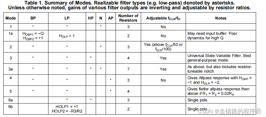
MF10-N是一个开关电容器(采样数据)滤波器。为了充分描述其传递函数,采用时域方法是合适的。由于这是很麻烦的,而且由于MF10-N非常接近连续滤波器,下面的讨论是基于众所周知的频域。每个MF10-N都可以产生一个完整的二阶函数。各种模式的特征总结见表1。
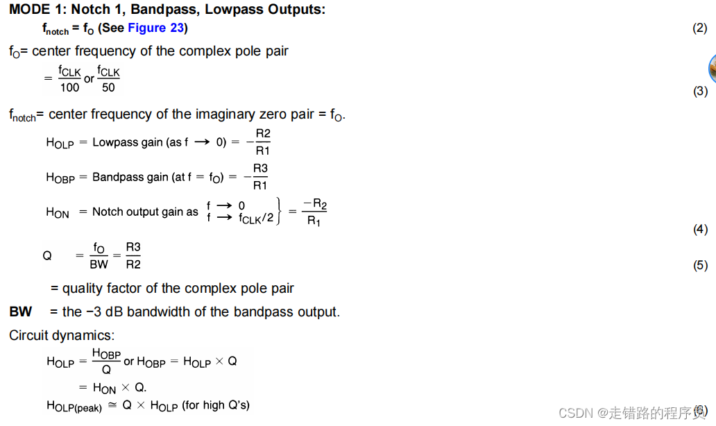
相关公式符号的定义.
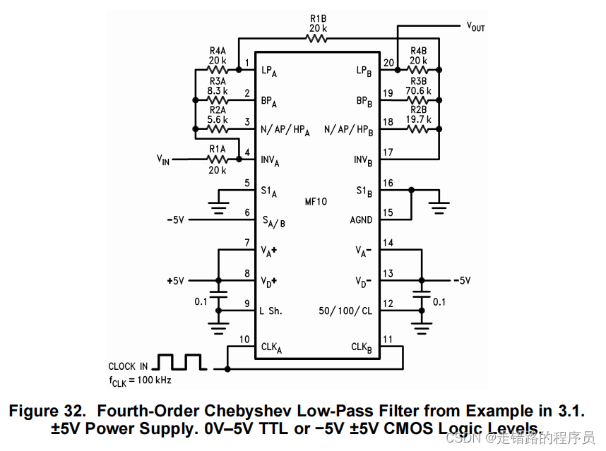
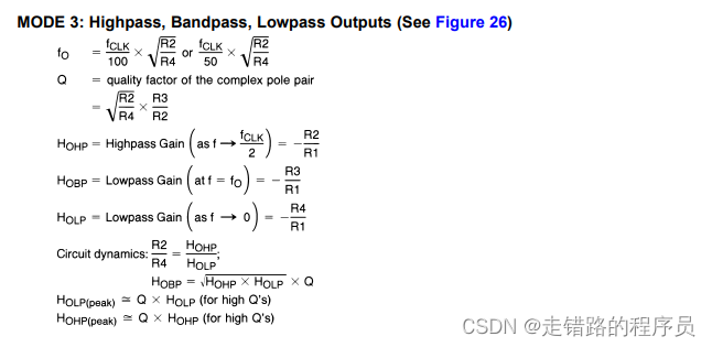
我的系统用的是模式三, 支持高通, 带通, 低通.电路图如下.

计算公式.
DESIGN EXAMPLE
In order to design a second-order filter section using the MF10-N, we must define the necessary values of three
parameters:
为了使用MF10-N设计一个二阶滤波器部分,我们必须定义三个参数的必要值:
f0, the filter section’s center frequency; 滤波器段的中心频率
H0, the passband gain; 通频带增益
Q. 滤波器的Q值
Q值对实际滤波效果影响倒不大,但Q值代表的是损耗 / 输入功率,Q值越高,说明损耗越大,意指会有部分能量在滤波器的电感上被损耗掉。在一般的低功率电源滤波器和信号滤波器上,此问题不会太突出。但在较大功率的滤波器上,这个损耗不可小视,一是会引起发热,发热后的电容会引起较大的负面影响,漏电流、耐压、容值等都会随温度变化而变化;二是耗电量大会导致无谓的电损失。
1、Q值得大小对扶贫特性在Ω=Ω0附近的影响较大
2、当Q=0.5时,成为Bessel滤波器,低通特性单调下降且通带较窄
3、当Q=1/根号 2=0.707时,幅频特性曲线最平坦 成为Butterworth滤波器
4、当Q=1时,称为Chebyshey滤波器
5、当Q>0.707时后,特性曲线将出现峰值,Q值越大,峰值越高
6、Q值太大,电路将趋向不稳定,此类电路最大Q值为6—8左右
These are determined by the characteristics required of the filter being designed.
这些都是由所设计的过滤器所需的特性所决定的
As an example, let’s assume that a system requires a fourth-order Chebyshev low-pass filter with 1 dB ripple,unity gain at DC, and 1000 Hz cutoff frequency. As the system order is four, it is realizable using both secondorder sections of an MF10-N. Many filter design texts include tables that list the characteristics (fO and Q) of each
of the second-order filter sections needed to synthesize a given higher-order filter. For the Chebyshev filter
defined above, such a table yields the following characteristics:
作为一个例子,我们假设一个系统需要一个四阶切比雪夫低通滤波器,直流统一增益,1000 Hz截止频率。由于系统的阶是4,它可以使用MF10-N的两个二阶部分来实现。许多滤波器设计文本包括列出合成一个给定的高阶滤波器所需的每个二阶滤波器部分的特征(fO和Q)的表。对于上面定义的切比雪夫过滤器,这样的表将产生以下特征:
f0A = 529 Hz   QA = 0.785
f0B = 993 Hz   QB = 3.559
For unity gain at DC, we also specify:
H0A = 1
H0B = 1
The desired clock-to-cutoff-frequency ratio for the overall filter of this example is 100 and a 100 kHz clock signal
is available. Note that the required center frequencies for the two second-order sections will not be obtainable
with clock-to-center-frequency ratios of 50 or 100. It will be necessary to adjust
本例的整体滤波器的时钟截止频率比是100,有fCLK = 100 kHz时钟信号。
fCLK = 100,000Hz
请注意,当时钟与中心的频率比为50或100时,将无法获得两个二阶部分所需的中心频率。这需要进行调整
100 = fCLK / f0
也就是说, 当时钟频率fCLK为100khz的时候, 中心频率f0 为1khz
externally. From Table 1, we see that Mode 3 can be used to produce a low-pass filter with resistor-adjustable center frequency.
在外部从表1中,我们可以看到,模式3可以用于产生一个具有电阻可调中心频率的低通滤波器。
In most filter designs involving multiple second-order stages,
在大多数涉及多个二阶阶段的过滤器设计中
it is best to place the stages with lower Q values ahead of stages with higher Q, especially when the higher Q is greater than 0.707.
最好将Q值较低的阶段放在Q值较高的阶段之前,特别是当较高的Q大于0.707时。
This is due to the higher
relative gain at the center frequency of a higher-Q stage.
这是由于在一个较高的q级的中心频率处有较高的相对增益
Placing a stage with lower Q ahead of a higher-Q stage
will provide some attenuation at the center frequency and thus help avoid clipping of signals near this frequency.
将低Q的级放置在高Q级的前面将在中心频率提供一些衰减,从而有助于避免该频率附近的信号被剪切
For this example, stage A has the lower Q (0.785) so it will be placed ahead of the other stage.
对于这个例子,阶段A有较低的Q(0.785),因此它将被放置在其他阶段的前面。
For the first section, we begin the design by choosing a convenient value for the input resistance: R1A = 20k. The
absolute value of the passband gain HOLPA is made equal to 1 by choosing R4A such that: R4A = −H_OLPA * R1A = R1A = 20k.
If the 50/100/CL pin is connected to mid-supply for nominal 100:1 clock-to-center-frequency ratio, we find R2A by:
对于第一部分,我们通过为输入电阻选择一个方便的值来开始设计: R1A = 20k。通过选择R4A = −H_OLPA * R1A = R1A = 20k. 使通带增益HOLPA的绝对值等于1。如果50/100/CL引脚以标称100:1时钟与中心频率比连接到中电源,我们发现R2A通过:

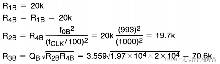
The resistors for the second section are found in a similar fashion:
第二部分的电阻器以类似的方式找到:
The complete circuit is shown in Figure 32 for split ±5V power supplies. Supply bypass capacitors are highly
recommended.
分裂±5V电源的完整电路如图32所示。强烈推荐使用供电旁路电容器。