版权声明:本文为博主原创文章,未经博主允许不得转载。 https://blog.csdn.net/IamSarah/article/details/76269737
这篇文章讲SPI总线,SPI是serial peripheral interface 的缩写,即串行外围设备接口。该接口是摩托罗拉公司提出的全双工同步通信的接口,该接口只有四根信号线,在芯片的管脚上只占用4根线,节约了芯片的管脚。
这四根信号信如下:
1、MOSI:主器件数据输出,从器件数据输入。
2、MISO:主器件数据输入,从器件数据输出。
3、SCLK:时钟线,有主器件控制。
4、CS:从器件的片选线,由主器件控制。
在点对点的通信当中:无须寻址工作,使用该接口实现全双工通信,高效简单,一个主器件可以连接多个从设备,每个从设备有独立的片选信号。不过该接口有一个缺点,就是没有应答机制。
该接口的工作机制:主设备启动,连接多个从设备,在sdo端输出,si端输入数据,均在sclk的上升沿传输数据,则经过8/16次时钟的改变,就能够完成8/16 bit的数据传输。
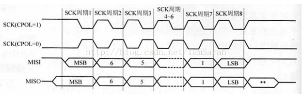
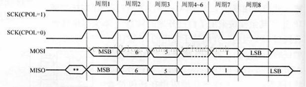
一般情况下,对有该接口的时钟会有两方面的设置:一方面是时钟极性,主要是用来规定空闲状态下sclk的值,0代表空闲状态下是低电平,1代表空闲状态下是高电平;另一方面是时钟相位的设置,主要是规定数据是在第一个跳变沿被采样还是第二个跳变沿被采样,0是代表第一个跳变沿,1是代表第二个跳变沿。下面两幅图给出不同相位下,不同极性的传输效果:
相位为0:
相位为1:
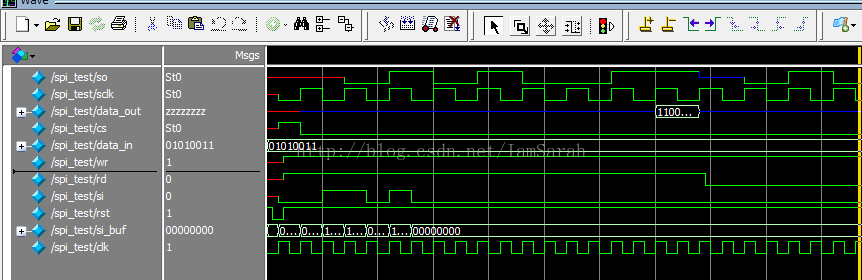
以上就是SPI接口的工作原理,下面给出其verilog实现,这里主器件用读命令和写命令来控制数据的输入和输出,并且对于一个字节的数据读和写分别用一个任务实现,如下:
module spi(clk,rd,wr,rst,data_in,si,so,sclk,cs,data_out);
parameter bit7=4'd0,bit6=4'd1,bit5=4'd2,bit4=4'd3,bit3=4'd4,bit2=4'd5,bit1=4'd6,bit0=4'd7,bit_end=4'd8;
parameter bit70=4'd0,bit60=4'd1,bit50=4'd2,bit40=4'd3,bit30=4'd4,bit20=4'd5,bit10=4'd6,bit00=4'd7,bit_end0=4'd8;

parameter size=8;
input clk,rst;
input wr,rd;//读写命令
input si;//spi数据输入端
input [size-1:0]data_in;//待发送的数据

output[size-1:0]data_out;//待接收的数据
output sclk;//spi中的时钟
output so;//spi的发送端
output cs;//片选信号

wire [size-1:0]data_out;
reg [size-1:0]dout_buf;
reg FF;
reg sclk;
reg so;
reg cs;


reg [3:0]send_state;//发送状态寄存器
reg [3:0]receive_state;//接收状态寄存器

always@(posedge clk)
begin
if(!rst)
begin
 sclk<=0;
 cs<=1;
 end
else
begin
 if(rd|wr)
 begin
 sclk<=~sclk;//当开始读或者写的时候,需要启动时钟
 cs<=0;
 end
 else
 begin
 sclk=0;
 cs<=1;
 end
end
end


always@(posedge sclk)//发送数据
begin
if(wr)
begin
send_state<=bit7;
send_data;
end
end

always@(posedge sclk)//接收数据
begin
if(rd)
begin
receive_state<=bit70;
FF<=0;
receive_data;
end
end

assign data_out=(FF==1)?dout_buf:8'hz;

task send_data;//发送数据任务
begin
case(send_state)
bit7:
     begin
	 so<=data_in[7];
	 send_state<=bit6;
	 end
bit6:
     begin
	 so<=data_in[6];
	 send_state<=bit5;
	 end
bit5:
     begin
	 so<=data_in[5];
	 send_state<=bit4;
	 end
bit4:
     begin
	 so<=data_in[4];
	 send_state<=bit3;
	 end
bit3:
     begin
	 so<=data_in[3];
	 send_state<=bit2;
	 end
bit2:
     begin
	 so<=data_in[2];
	 send_state<=bit1;
	 end
bit1:
     begin
	 so<=data_in[1];
	 send_state<=bit0;
	 end
bit0:
     begin
	 so<=data_in[0];
	 send_state<=bit_end;
	 end
bit_end:
     begin
	 so=1'bz;
	 send_state<=bit7;
	 end
endcase
end
endtask

task receive_data;
begin
case (receive_state)
bit70:
      begin
	  dout_buf[7]<=si;
	  receive_state<=bit60;
	  end
bit60:
      begin
	  dout_buf[6]<=si;
	  receive_state<=bit50;
	  end
bit50:
      begin
	  dout_buf[5]<=si;
	  receive_state<=bit40;
	  end
bit40:
      begin
	   dout_buf[4]<=si;
	  receive_state<=bit30;
	  end
bit30:
      begin
	  dout_buf[3]<=si;
	  receive_state<=bit20;
	  end
bit20:
      begin
	  dout_buf[2]<=si;
	  receive_state<=bit10;
	  end
bit10:
      begin
	  dout_buf[1]<=si;
	  receive_state<=bit00;
	  end
bit00:
      begin
	  dout_buf[0]<=si;
	  receive_state<=bit_end;
	  FF<=1;
	  end
bit_end0:
      begin
	  dout_buf<=8'hzz;
	  receive_state<=bit70;
	  end
endcase
end
endtask
endmodule
`timescale 1ns/1ns
`define half_period 10
module spi_test;
parameter size=8;
wire so;
wire sclk;
wire [size-1:0]data_out;
wire cs;

reg [size-1:0]data_in;
reg wr,rd;
reg si;

reg rst;
reg [size-1:0]si_buf;
reg clk;

always#(`half_period) clk=~clk;
initial
begin
clk=0;
rst=1;
si_buf=8'b1001_1010;
data_in=8'b0101_0011;
#5
rst=0;
#10
rst=1;
wr=1;
rd=1;
#380 rd=0;
#1000 $stop;
end
always@(posedge clk)
begin
si_buf=si_buf<<1;
si<=si_buf[7];

end

spi m(clk,rd,wr,rst,data_in,si,so,sclk,cs,data_out);
endmodule